Bias-assisted indium mass transport on nanotube surfaces (Jump-start Project)
Collaborator: Marvin L. Cohen, UC Berkeley
The development of robust experimental techniques for manipulating and delivering nanoscale material is of extreme importance for realizing much of the promise of nanotechnology. Recently, experiments in Prof. Alex Zettl’s group at UC-Berkeley demonstrated controllable, reversible mass transport along the surface of multiwalled carbon nanotubes (MWCNTs) . Indium nanocrystals deposited on MWCNTs exchange atoms with neighboring nanocrystals along the tube with an applied voltage.
The direction of In adatom transport is reported to be determined by the sign of the voltage bias, with the In atoms always moving towards the cathode. This phenomenon is similar to electromigration of metals on semiconductor surfaces. Robust nucleation sites on the surface of the MWCNTs are observed, suggesting preferred locations for particle growth on the surface. As the voltage bias is cycled, the In adatoms return to nucleate nanoparticles at the same sites each time.
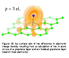
In an effort to understand this behavior, first-principles calculations of indium adsorption on graphene were performed in order to understand indium diffusion on carbon and boron nitride nanotube surfaces. The adsorption energy was computed as a function of In coverage, and for low surface densities, In adatoms become positively charged by donating about one electron to the surface (Figure 14). This is consistent with experimental observations of bias-assisted indium flux in the direction opposite to that of electron flow.
Publication arising from this work: F.J. Ribeiro, J.B. Neaton, S.G. Louie, and M.L. Cohen, "Mechanism for bias-assisted mass transport of indium on carbon nanotube surfaces," Physical Review B 72 (7), p.75302, (2005).


