

Electronic structure calculations of tapered silicon nanowires
Nanowires are often observed to be tapered rather than straight-edged, with diameters (d) shrinking by as much as 1 angstrom per 10 angstroms of vertical growth, depending on the synthesis technique and conditions . However, most theoretical work to understand the electronic, optical, and structural properties of nanowires have assumed a straight-edge geometry. It is well known that the optical gaps of nanowires are larger than bulk due to quantum confinement effects, and that the gap increases with the diameter . In addition, the electronic structure of nanowires depends upon the surface geometry . In a tapered nanowire, the nature of the confinement changes along the axis direction, and the surface is stepped. It is therefore of fundamental interest to study how this morphology impacts their electronic structures.
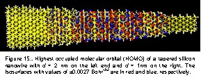
In this work, we are investigating properties of tapered nanowires with ab initio calculations using a local-orbital basis. We are studying tapered hydrogen-passivated silicon nanowires along [011] direction, with length l = 10 nm, and d varying from 1 nm to 2 nm. For comparison, we also calculate straight nanowires with the same length and d = 1 and 2 nm, respectively.
Thus far, the following preliminary results have been obtained. Examining the electron density of states (DOS) of selected layers in the tapered wire, we find that the band gap of individual layers increases along the axis direction with decreasing d. On the other hand, in straight wires the DOS are similar at different layers (except for the top and bottom layers), and the fundamental gap hardly changes, as expected.